Today’s complex PCBs are being packed with a boatload of tiny components and are designed to run at ever-increasing speeds. So it certainly comes as no surprise to hear that silkscreen legends are fairly low on the designer’s priorities for consideration. However, the silkscreen’s function—that of aiding the manufacturer and engineer to locate components on the board—remains important.But just how important is it that all components be labeled individually, especially on boards so densely packed? With automated assembly processes and the widespread use of electronic documentation, certain tradeoffs can now be made, where individual component identification is sacrificed for other types of identifiers. So in the spirit of endeavoring to design the best silkscreen possible, I will review the three types of silkscreen technologies and then advocate a more rational approach to today’s silkscreened boards.Component densities, along with package miniaturization, have become the main culprits in driving technology forward in both the fabrication and assembly processes. This is nowhere more evident than in the major advances in the fabrication realm in which High Density Interconnects (HDI), e.g., blind and buried vias, are now commonplace on most designs. And while certainly not as impressive as the move toward HDI, advances have also been made in how non-conductive ink is applied to create the silkscreen legend.
The board lettering that we call the “silkscreen” originally derived its name from the process of using a stencil to apply ink to the finished raw PCB, in much the same way that lettering or a graphic design is applied to T-shirts. Although this method is still used, new and improved processes are used today that significantly increase both throughput and legibility. Depending on the specific fabrication vendor and the specific make-up (text height and text-pad clearance) of the silkscreen input, one of three methodologies is used to apply the ink to the board:
Manual screen printing: This is the original silkscreening process, in which epoxy ink is pushed through a nylon screen stencil onto the laminate, which is then baked to cure. It is the least precise method of applying legend to a PCB.
Liquid Photo Imaging (LPI): A liquid photoimageable epoxy is coated onto the laminate, exposed with UV light through artwork, developed, and then baked to cure. This process is much the same as the soldermask process earlier in the board’s manufacture, but using (usually) white material instead of the (usual) green color of the soldermask.
Direct Legend Printing (DLP): This method is most analogous to the familiar process of printing documents on paper. Acrylic ink is applied onto the raw PCB directly from CAD data using a very accurate, high-end inkjet printer. As the ink is printed, it is instantly cured with UV light.
Chart 1, below, shows the various pros and cons of these three methods, along with DFM considerations.
 From the standpoint of being able to reduce the text size and clearance to component pads and still be legible, the DLP process certainly gives the designer a better shot at packing in more component reference designators and other markings than the other two processes. The two roadblocks for the designer are availability and applicability. Not all fabricators have DLP printers, and for some applications the acrylic ink is not a viable option due to out-gassing (e.g., for space applications) or for PCBs with silver finishes. The question that has to be asked is: How small can you go and still be able to read the text with the naked eye? I would venture to say that unless we are all willing to use magnifiers, the DLP technology with .020″ minimum text sizes is pretty much at the limit of what can be sensibly achieved as useful. As a point of comparison, most printed material uses a font size of between 8- and 12-pt. (1 pt. = 1/72″). Silkscreen text at .050″ high is less than 4pt. type, while silkscreen labeling at .025″ high—which is the preferred minimum height for DLP—is like trying to read less than 2pt. type!
![Download Optimum's Designer Handbook! [PDF format]](https://www.optimumdesign.com/hs-fs/hub/317720/hub_generated/resized/3f81ff4e-f8cf-4a7b-8bfb-a62958faa41a.png)
In the assembly process, a well-designed silkscreen is useful during all phases of the various inspection processes. The ease and speed at which inspectors are able to accurately identify polarity markings and component locations can reduce both costs (time=money) and the likelihood of errors occurring. This applies not only to the assembly process but is equally or even of greater value for the engineer and technician in the lab during bring-up, debug, and rework phases. The easy accessibility of CAD viewers to read in files such as ODB++, searchable assembly drawings, and CAD databases now aid both manufacturer and engineer to quickly search for components which in the past were much easier to find on the physical PCBs.
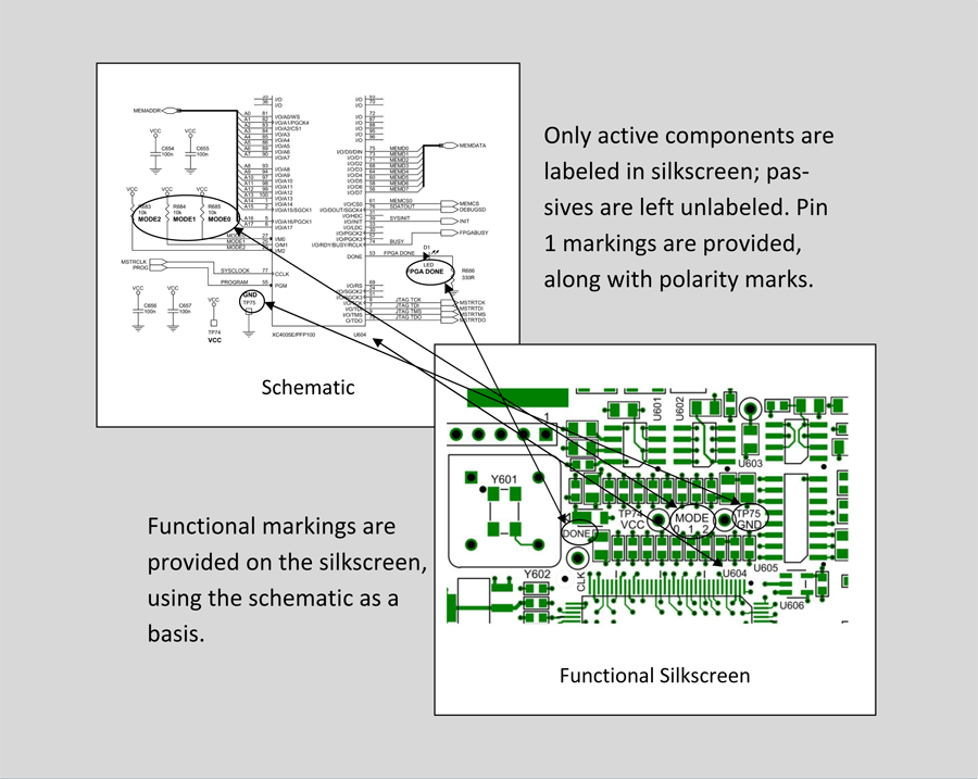
For these reasons, uniquely identifying all the components on a PC board is no longer necessary or, in some cases, even possible. In particular, passive components, which make up the bulk of devices on a board, need not be identified. Instead of telling us what each individual component is, what we need our silkscreens to tell us is: Circuit functionality. This would involve labeling what a circuit does rather than its components. Circuit function labeling is much more useful to the engineer, and much more achievable on a packed PCB. Examples of circuit function labeling are configuration and option settings, such as resistor Mode and Select (MODE0, -1, -2 or SEL0, -1, -2), and testpoints, LEDs, and jumpers. The labeling can be anything that the engineer deems important. Of course, active components would still be labeled with reference designators, as well as Pin 1 designations and polarity marks, but the idea of circuit function labeling is to substitute hundreds or even thousands of passive reference designators, many of which cannot be easily read, with only items important and useful to assembly, inspection, and test. The simple reality is that it’s just not feasible or possible in many cases to fit everything onto the silkscreen that you would like, especially considering that reference designators can often be two to five times larger than the component package it represents. With a firm understanding of the manufacturing and debug requirements, the designer and engineer can work together to make the best practical tradeoffs of component identification vs. circuit function for high component density boards. By doing this, it will result in a silkscreen legend that is legible and functionally useful for both assembler and engineer.