
Mentor’s Display Control gives designers and librarians myriad options for influencing how a design is displayed on the screen....
READ MORE
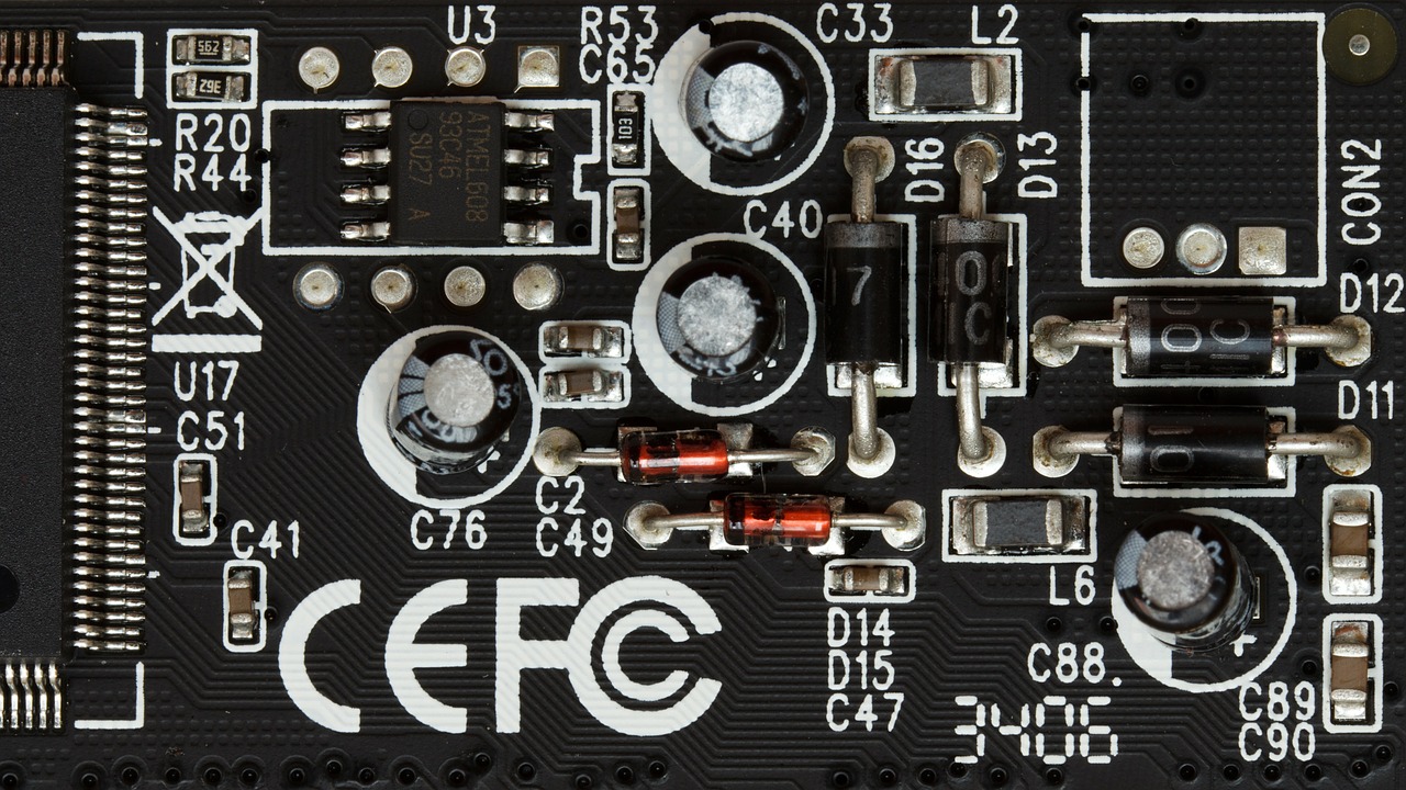

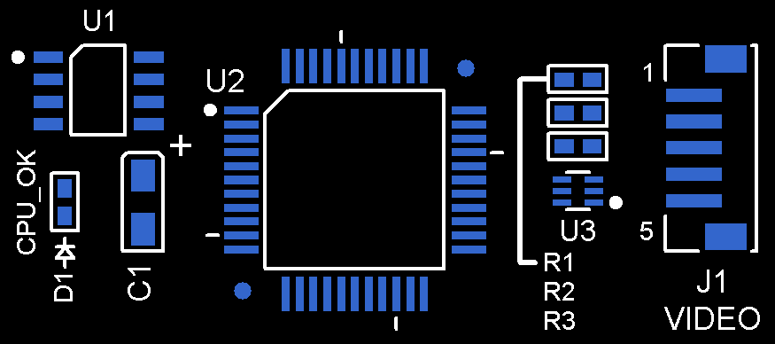
The silkscreen is a helpful tool in identifying components on the board. During PCB layout it should be designed for a consistent flow that allows easy identification of parts while using a minimum of leaders in difficult areas. Special care should be taken to ensure that each device has its appropriate associated markings, such as polarity, pin #1 location, 10th pin marker for fine pitch parts, or connector pinouts. Some parts may require additional labeling that should be specified by the customer. This may include labeling connectors, LEDs, switches, high voltage areas, or critical circuits (see the figure below).
Silkscreen Markings and Clean Up
Text on each board design should be clear and consistent. Letters must not cover surface-mounted land pads, nor should they overlap other text or silkscreen outlines. Some common mistakes to be avoided during cleanup include placing silkscreen text over etched text, on top of fiducials which include an enlarged soldermask opening, and any cutouts or milled areas. It is also best practice to view the Soldermask layer when cleaning up the Silkscreen, so as to avoid these common mistakes.
![Download Optimum's Designer Handbook! [PDF format]](https://no-cache.hubspot.com/cta/default/317720/240d1413-c945-4cb8-a546-a84937b16039.png)
Only two text rotations are allowed on the board: 0and 90(unless otherwise specified).
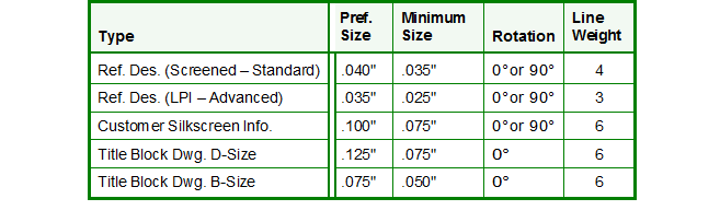 Text Size/Rotation shows standard sizes, spacing and styles for text.