Symbols are the second major portion of any PCB library. Electrical symbols show the connection between parts, and are utilized...
READ MORE


Organizing your parts into partitions based on part type is a major step in organizing your library, but properly labeling each component in a partition is also critical for rapid identification. A part in your library’s labeling information should include everything necessary for a user to identify the part. Let’s take a look at how various components in the Optimum Library are named.
Footprint Naming
Optimum’s footprint naming standard is based on IPC7351B naming conventions for SMD components. Some additional conventions have been added, as IPC standards have some limitations. First let’s take a look at the baseline rules for naming footprints.
- Units of Measure - Dimensions are defined using the metric system. In some instances, imperial (inch) units may be appended to the land pattern name. This is done to reduce confusion between the metric dimension and the commonly used industry name. Each component naming convention will have the resolution defined in its description. An example is the metric 0603, which is commonly known as an industry 0201.
- Leading and Trailing Zeros - Leading zeros are not required. Trailing zeros are required to meet the components resolution definition.
- Land pattern name length will be a maximum of 31 characters.
- Typographical Conventions:
- The _ (underscore) is used as a separator between different fields of a land pattern name. The underscore may also be used in place of the period (.) character.
- The – IPC uses the dash as a separator for the pin quantity field, the dash is replaced by an underscore in this library for this purpose. The dash is also used within the pin quantity to determine missing numbers of pins, i.e. 24-28 indicates a 28 pin package in which only 24 pins are used.
- The X (uppercase letter X) is used between dimensions. lengthXwidthXheight.
- The M, N, L, and Q suffixes are to appear at the end of every common SMD land pattern name. They represent Maximum, Nominal, and Least land size conditions, respectively. This rule excludes BGA packaged land patterns where only nominal is defined. The Q suffix denotes that the manufacturer recommended land pattern has been used for the land pattern.
- THROUGH-HOLE components do not use a density level suffix.
- The () is used to denote required information to be added to the naming convention.
- The [] is used to denote optional information to be added to the naming convention.
- Only alpha-numeric characters, such as, underscores (_), and dashes”-“ are acceptable characters.
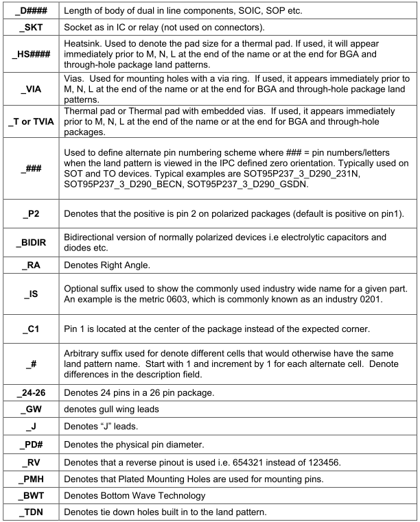
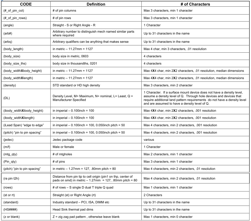
- Defined Suffixes – The suffixes in the following table have been defined for various different component types.
Defined Suffixes
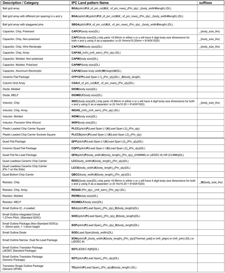
IPC Naming Convention Table
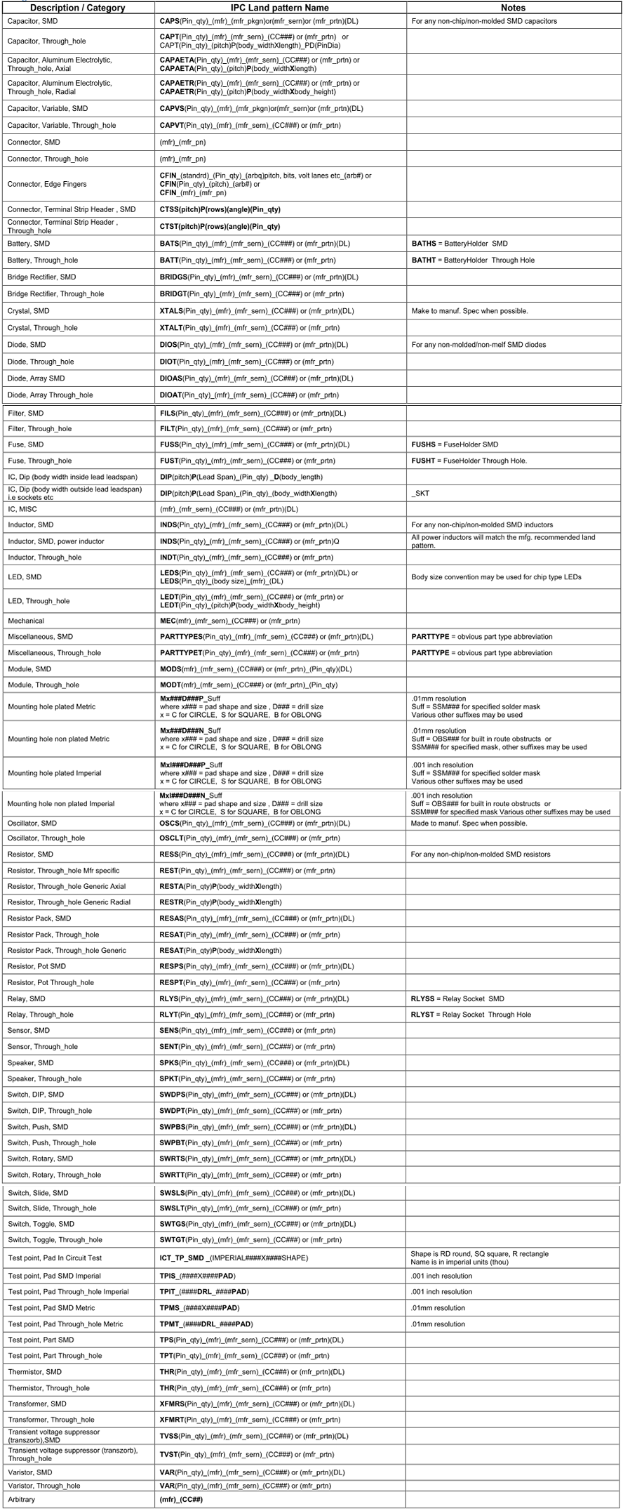
Non IPC Naming Convention Table
Naming Convention Codes
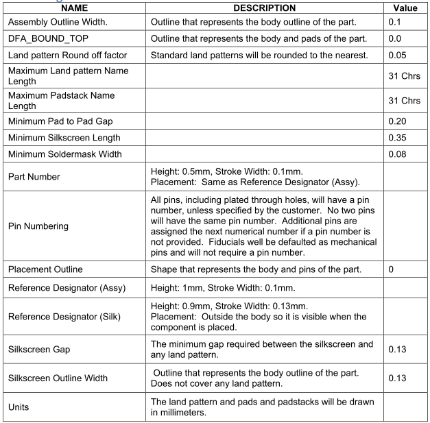
Default Settings
Generic Components
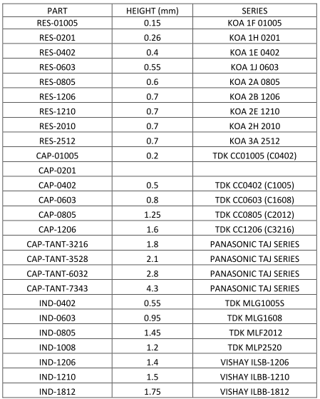
Many resistors, capacitors, and inductors will be included in a library. A best practice is to leave these components within the library in generic form, meaning they have no manufacturer part number associated with the footprint. Lack of MPN means height measurements do not exist, so heights for these components is based on the following sources.
Chip Resistors: Heights based on KOA RK73B series.
Chip Capacitors: Heights based on TDK “C” series.
Generic chip Tantalum Capacitors: Heights based on Panasonic TAJ series.
Generic chip Inductors: Height based on TDK MLG and Vishay ISLB series.