
Isolate In X/Y Axis
Because this is a mixed signal design, we need to pay careful attention to how we will isolate these different circuit types from each other. The easiest way is to do the simple X/Y axis isolation, by defining different areas of the board for different circuit types. This works well when the density, particularly in digital circuits, is low enough and the separation between circuit types is very clearly defined.
When this method of isolation is used it is common, although seen by some as unnecessary, to have a slot in the ground and power planes with a bridge area where the zones are joined and all digital control signals for the RF circuitry must be routed over this bridge.
Many electrical engineers and layout designers prefer to never use slotted or isolated ground planes. It can be argued that, if the design is placed and routed in the proper manner, then slots in the planes have no beneficial effect. This is because the high-speed signal return currents will flow in the ground plane adjacent to the signal path and will be directly under or over the signal path itself (the path of least impedance), and will therefore not be circulating in other areas.
When a board is designed without slotted or isolated planes, then the slot areas shown in Figure 1 are seen simply as ‘borders’ or ‘no go zones’ for routing. When slotted or split planes are used, all connections between the digital and RF zones must be routed over the ‘bridge’. There will be times when the electrical engineer or customer demands that the planes be slotted. This should not present a problem as split, slotted and solid planes can be used effectively so long as the solid plane methodology still essentially respects the no go zone where the slot would be.
![Download Optimum's Designer Handbook! [PDF format]](https://www.optimumdesign.com/hs-fs/hub/317720/hub_generated/resized/3f81ff4e-f8cf-4a7b-8bfb-a62958faa41a.png)
This means that different circuit areas should be visualized as being separated by slots or splits, even when a solid plane is used, and those visualized separations are seen as no go zones for routing. This methodology helps to contain digital and analog routing in their own respective zones which is more than enough to ensure proper isolation.
The following stackups and descriptions are based on the presence of slots or splits in planes to isolate analog and digital zones, since it is recognized that this is still the method used by most layout designers. The same information holds true for layout designers who do not use slots or splits in planes as long as the above visualization is employed.
Figure 1 (floorplan view) and Figure 2 (cross section view) are an example of X/Y zone isolation.
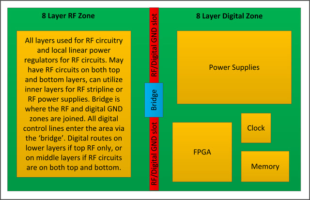
Figure 1. Floorplan View Of X/Y Axis RF And Digital Zone Isolation

Figure 2. Cross Section View X/Y Axis Only RF And Digital Zone Isolation
Notes X/Y axis isolation:
- The slot area in Figure 1 and Figure 2 does not have to be a physical slot cut out of the board, it may also be a copper layer slot, or moat, used to divide the RF and digital ground zones. The slot is generally bridged on a ground plane in a single location, and this is where the digital signals cross into the RF zone, they must be routed over the ground bridge so the return current for these signals will flow back to the digital ground zone via this ground bridge. With careful design the slot can simply be a no go zone for anything other than ground between the two circuit types and the planes can be solid.
- When X/Y only isolation is used, it is best to try to organize the placement such that any low speed digital control signals that transition between digital and RF zones actually route as little as possible into the RF zone. Try to locate components in such a way that the digital control pins are close to the bridge between the zones. This will minimize digital return currents in the RF zone. Layer 6 in Figure 8 above shows digital signal routes in the RF zone. In practice, these should penetrate the RF zone little as possible and the remainder of layer 6 should be a ground flood in the RF zone. When the ground flood is applied, the coplanar distance to any digital signals should be defined as 10H or more, where H is the smaller of the dielectric thicknesses between layer 5 and layer 6 and between layer 6 and layer7. This flood serves to improve noise suppression in the RF zone and also to ensure copper balance in the design all through the Z axis, empty layers or large void areas will tend to cause warping in the final circuit board.
- This method of isolation works well when the digital signals are essentially static controls and/or they penetrate the RF zone as little as possible. If this isolation method is used with longer, higher density digital signals or fewer but higher speed edge rate digital signals, then there will be a danger of injecting significant digital noise in the RF ground planes, and thereby compromising the RF functionality. With higher density or higher speed digital signals it is better to split the design in BOTH X/Y and Z axes.


