Have you ever started a switching power supply layout, only to realize that it is impossible to match the datasheet’s suggested layout? Have you wondered which parts of the reference design you should maintain, and which parts you could change? How do layout choices affect the switcher’s performance? In this article I intend to briefly tell the history, explain the major workings, and provide examples of switching power supplies and their design techniques. My hope in doing so is to convey the enjoyment I get from designing these unique circuits.
Switcher History
Some may think that the use of switching power supplies began in the 1970s, but the principles were known as early as the 1930s. Implementations of them include the IBM 704 mainframe computer (1950s), the NASA Telstar satellite (1960s), and Apple’s famous Apple II personal computer (1970s). And pretty much ever since then…well, it was on!
There is no lack of those who want to take credit for the switching power supply’s popularity. However, the reality is that innovations in the semiconductor industry (improvements in switching transistors and the development of new controller ICs) are what should be credited with the explosion of their popularity. A power switch that allowed for very fast switching of large currents was really the key to making switching power supplies practical for the wide array of uses we see them in today. The invention of the Vertical Metal Oxide Semiconductor (VMOS) power switch is what provided this capability. Bipolar transistor power switches work well in high-power switching applications, but these components exhibit slower switching characteristics than the MOSFET, a VMOS power switch. It was important, especially for consumer electronics applications, to increase the switching speed, not just for power efficiency, but also to be above the audible frequency range.
Switcher Terminology
A switching power supply is also known by other names. The term switchmode power supply was widely used until Motorola starting enforcing their SWITCHMODE™ trademark.
“Switched mode” and “switching mode” are now common terms, as well as the initials SMPS. In a computer, the main power supply may be called a switching power supply, while point-of-load supplies may be called switching regulators. To eliminate confusion, the universal term “switcher” will be used in lieu of all of these.
![Download Optimum's Designer Handbook! [PDF format]](https://www.optimumdesign.com/hs-fs/hub/317720/hub_generated/resized/3f81ff4e-f8cf-4a7b-8bfb-a62958faa41a.png)
Switcher Operation
A switcher uses a power switch, filter capacitors, magnetics, and a rectifier to transfer energy from input to output, providing a regulated voltage source. It works by rapidly turning the power switch on and off. The input voltage and the duty cycle, which is the proportion of time the switch is on vs. off, determine the output voltage. During the ON state, the switch is in saturation mode with negligible voltage drop across it. During the OFF state, the switch is in cut-off mode with negligible current through it. These are two very efficient states, in which the power switch dissipates very little power. This results in very efficient power conversion and very little power loss due to heat.
Switchers do not require low-frequency transformers, which are large and heavy; however, they do require high-frequency filtering. The filtering can be performed using much smaller components. All of this gives switchers a huge advantage over their linear regulator counterparts in the areas of miniaturization and power efficiency. The disadvantages of using a switcher are that they can be demanding in layout and, because of the fast switching and high current paths, can radiate EMI (they can be noisy!).

Switcher Types
There are two types of switchers: transformer isolated and non-isolated. Switchers using input voltages above 42.5 VDC typically require the use of transformer isolation. Non-isolated switchers can be very small and compact, and often the power switch and control circuitry reside on one chip. Different switcher topologies (electrical arrangement of the switch, magnetics, capacitors, and diode) exist for fulfilling the source and load voltage requirements of today’s electronic devices. Table 1 lists three common non-isolated switcher topologies.
Isolated switchers have many common topologies. Each has characteristics that make it more suitable for a specific power supply application. Input voltage, output power, and maximum output current are major factors when selecting a topology. Other factors include cost, efficiency, number of outputs, isolation, size, and engineering requirements. Isolated switcher topologies can be fairly complex, but their basic design is based on non-isolated switcher topologies. The inductor in a non-isolated switcher design is split and coupled, forming a transformer, which provides the isolation. Using this concept, a Forward Converter is based on the Buck Converter, and the Flyback Converter is based on the Buck-Boost. The remaining listed isolated topologies (Table 2) are derived from the basic Forward Converter design.
For the purpose of simplicity, this article will focus on the non-isolated, DC-DC, single positive output, step-down regulator (also known as the buck converter) as an example of a switcher layout.

Layout hints
The best resource when beginning a switcher layout is the manufacturer’s datasheet, along with any application notes. Possibly the layout provided for evaluation purposes can be used as a reference. Generally, if you precisely follow the recommended layout and notes, then the resulting layout performs as well as the manufacturer intends it to. More often than not, however, one or more factors will force you to make changes to your implementation of the reference layout. These factors include:
The major components are different in size and shape
Circuit functions omitted or added
Mechanical restrictions
Proximity to other circuits and board density
Additional thermal requirements
Test requirements
Fine pitch parts requiring thinner copper weight
Larger vias required due to board thickness or reliability concerns
Different number of PCB layers
Any of these factors may affect your ability to implement a manufacturer’s layout in your design. This means something has to change, but what? And what if there is no application note to turn to? How do you make good decisions on the design of such a critical circuit?
Circuit Overview
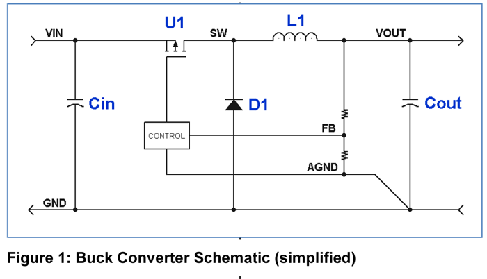
The first thing is to identify the key power components in the switcher circuit. These are (reference the schematic in Figure 1):
Filter capacitors: Cin and Cout quickly source and sink large levels of AC current.
Power switch: U1, the series pass element, is usually MOSFET. It may be one or more discrete devices, or built into the controller, if present.
Inductor: L1, the magnetic element, provides storage for energy that will be recovered while the switch is off.
Diode: D1, the output rectifier, is usually a Schottky diode, but in ultra-efficient (e.g., synchronous rectifier) switcher designs, this function will be performed by a MOSFET.
The inductor and Cout capacitor form an LC filter, providing high-frequency voltage-ripple filtering. Sometimes, there is a high-frequency bypass capacitor (Cbypass or Chf) connected in parallel with Cin. This capacitor needs to be placed very close to the switch input. Often the power components for a switcher layout are “on-chip”, that is, they reside on the controller. The PCB routing will follow the same rules as when these components are “off-chip.”
Power Paths
Understanding how the switcher works requires us to identify the multiple critical current loops, DC (continuous) and AC (alternating).

The DC current loops are 1) the Input Loop, from the input source, through the capacitor Cin, and returning to the source, and 2) the Output Loop, from the capacitor Cout, through the output load, and returning back to Cout. Figure 2 shows the locations of the Input and Output loops. These loops need to be connected both directly at their respective filter capacitor’s terminals, and with short, wide traces for low impedance.
These two separate DC loops can be thought of as the current flow paths of the unregulated source, and the regulated load voltages.
The AC current loops are the Power Switch Loop and the Output Rectifier Loop.
The power switch loop is formed while the power switch is ON. During this time, the forward current flows from Cin, through the switch, the inductor, through Cout and returns back to Cin.
The output rectifier loop is formed while the switch is OFF. Now energy is recovered from the inductor (magnetic storage). During this cycle, the forward current flows from the inductor to Cout, and returns from Cout through the rectifier and back to the inductor.
It may help to think of a switcher’s function as converting DC at its input into AC and then back to DC at its output, for the purpose of power efficiency.
The AC current loops are the most critical connections in any switcher layout. These paths take priority over all others. Their placement and routing need to be planned first and they need to be routed with short, low inductance paths (see Figure 3).

The AC current return paths should be matched to the respective forward current paths as much as possible. The best way to do this is to use a full ground plane in close proximity on the next adjacent PCB layer. By minimizing the loop area and making the return path closely follow the forward current path, the opposing magnetic fields will tend to cancel each other out. This reduces unwanted EMI. The return path should not be occupied with too many non-ground vias, which could undermine the effective copper for this path by creating openings or slots in this plane. It is also best to line up these vias, leaving wide alleyways of copper in the direction of the return path. The difference of the two AC current return paths (from the anode of the rectifier to the negative terminal of Cin) should be a short, low impedance, common point ground connection that includes the negative terminal of Cout and, if applicable, the controller thermal pad and any PGND connections.
All power components should be located on the same side of the board, and forward current path connections should be made without thermal relief and without the use of vias. The ground vias should also be connected to the plane without thermal relief.
The output of the switch is called the SW node, and is part of the forward AC current path. It carries the fast-switching, high-amplitude voltage swings (high dV/dT), along with high peak currents. This connection in particular needs to be as short as possible. It is important at the controller level to make this connection very low inductance, and it should be wide enough for the current flowing through it. Widening the connection to compensate for a longer distance is not recommended. This is because the likelihood of this connection becoming an antenna and radiating EMI is directly related to its length. The switcher circuitry should be placed in such a way that this connection is kept away from other circuitry, including other switchers on the same board.
The SW node connection should not be part of the copper flooding that is used to help dissipate heat, even if it is the best mechanical way to extract heat from the switcher (see Figure 4). Copper flooding for thermal management should utilize the low impedance and quiet DC connections (GND, VOUT, and VIN). Air flow direction may also need to be examined when placing tall components, like the inductor and filter capacitors, around discrete power switches. The compact size of a switcher layout, which is necessary to reduce EMI, can also make effective heat extraction a challenge.
Control Circuitry
The final aspect of switchers that we will look at is the control circuitry. The control circuitry is what determines the duty cycle, which, in turn, determines the output voltage. The duty cycle control signal, which may be provided by either a fully integrated power supply controller or by a simpler gate driver, carries the switching frequency (see Figure 4). This trace carries medium-size current, and it should be routed away from the high-current loops. It should also be routed away from any sensitive circuitry that it could affect. It may also be required to route this signal as a pair with another signal, from the driver output to the power switch, in order to reduce the loop area and to provide common mode noise rejection.

Duty cycle is calculated to ensure that the switcher provides the intended output voltage. To correctly adjust the duty cycle, some form of feedback from the output load is needed: either voltage or current. Analog error-correcting amplifier circuitry is often used for this purpose. The input to this amplifier (FB node) is high impedance and, therefore, sensitive to noise, so the connection to it should be very short (see Figure 5). To accomplish this, all components that generate the feedback signal (for example, a voltage divider network), should be placed close to the controller, with the input to these components routed to the last output capacitor or sometimes the load. The challenge is to keep the FB signal and other low-level analog control signals from being corrupted by the high dV/dT power paths, while still being in close proximity to them. For this reason, many times you will need to provide a separate analog ground plane area where these low-level signals are referenced, and which is connected to ground at a single point. Feedback traces and all analog signals should cross into the analog ground area at this common point.

Summary
Some datasheets or application notes may be followed exactly, if the layout they provide is perfect for dropping into your design unchanged. This is rarely the case with switching power supplies. Whether it is a function that is added or omitted in the schematic, or a component that is too large for the space provided, or something as small as a change in via size, something will need to be different on your design. But with such a commonly used circuit that can so easily radiate EMI due to the fast changes in voltage and current, the designer needs a deeper understanding of switcher operation in order to complete the layout successfully. I hope the information above will prove helpful to you in making those necessary decisions in your PCB designs. This article has only scratched the surface of the vast topic of switcher layout. Some of the discussion here will be pertinent to your layout, while some may not be. This is because, while sharing a common switching principle, each switcher application is unique. But I believe this can be what makes a switcher layout so much fun.


