
Integration is the process of adding intelligence to the PCB database by means of a netlist or schematic. This can only occur...
READ MORE

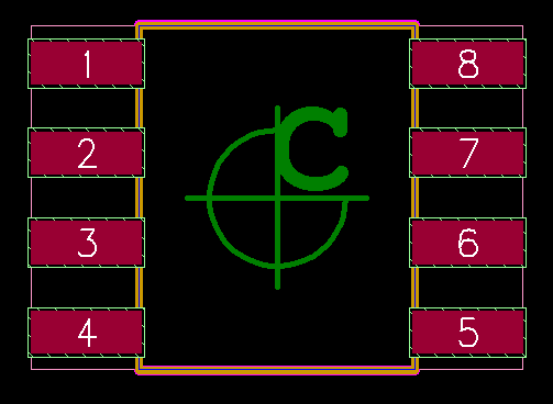
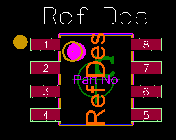
Building a component library for your PCB designs is a painstaking process. Ensuring that all of your parts are perfectly accurate is critical to an error-free design and assembly process. There are a number of different layers and properties which must be included in each PCB footprint in order for the part to be complete. Let’s take a look at a standard 8 pin IC to see what’s included.
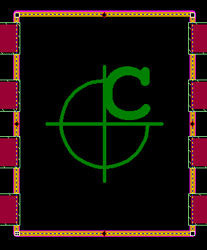
Placement Outline
This outline surrounds the entire body of the component, and is the primary layer responsible for defining the shape of the part. Height information for the component will also be included in the Placement Outline, accessible by selecting the placement outline, right-clicking it, and selecting Properties.
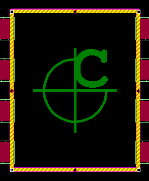
Assembly Outline
The assembly outline represents the physical body of the component, not including Pin to Pin. The physical casing of any component is represented by the Assembly outline. In many instances the Assembly Outline will be identical to the Placement Outline.

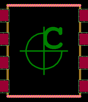
Silkscreen Outline
This layer will become the silkscreen once the board moves to assembly. When possible, the silkscreen outline should be an exact copy of the assembly outline. On smaller components like SOTs, resistors and capacitors, etc, the silkscreen layer should surround the entire body of the component. It is critical that the silkscreen layer not overlap with the pads of the component, which is why the two horizontal lines at the top and bottom of the component are the only silk screening present.
DFA_Bound_Top
The DFA bound layer is used in Design For Assembly in order to check clearances between components. It is necessary that the DFA Bound Top layer surround the entire body of the component. In many instances this layer will be identical to the placement outline.
Other Modifications
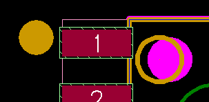
Different companies will have different requirements for various modifications to a footprint. The corner of the assembly & silkscreen outlines nearest pin 1 should be chamfered. This allows for easy component orientation identification in the assembly process. A dot should also be placed on the silkscreen & assembly layers, adjacent to pin 1, for similar identification purposes.
Part Labeling
Once pin 1 identifiers and other part modifications have been added, the final step is to include part labeling for the component. At Optimum that means a Reference Designator, as well as an Assembly layer Reference Designator. A part number on the Silkscreen layer is also included.
It seems like a lot, but ensuring that all of those elements are present within the parts you build is critical from an accuracy perspective. Another essential library process not expounded upon here is how to most accurately check the components that you've made. Stay tuned to the Optimum blog for a look into our library part checking process.